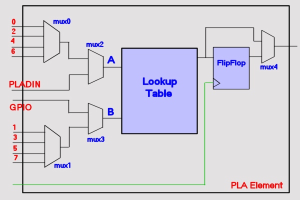
As mentioned each block is made up of 8 elements. Each of these elements is identical, consisting of a serious of muxes and a 2-input lookup table. This lookup table can be used to generate any output based on 2 inputs e.g. AND/OR/NAND etc. The diagram below shows the structure of the elements.
The elements are connected together by means of a feedback bus i.e. the output of each element
is connected to a bus, an element can then take inputs from this same bus thus allowing it access to the outputs of each of the other elements. This
arrangement is described further in the section on "blocks 0
& 1". The diagram shows mux0 and mux1 taking inputs from the other
elements. Mux0 takes inputs from elements 0,2,4,6 and so is called the even
mux. Similarly mux1 recieves inputs from elements 1,3,5,7 and is referred to as
the odd mux.
As well as the inputs from the other elements, the user can also select an input
from either the PLADIN register or the GPIO pins. These can be seen connected to mux2
and mux3 respectively. Once the user has chosen their input(s) to the lookup
table they must then select which function to apply to them. In the PLA Tool
this is accomplished by choosing from a predefined collection of functions
presented in a drop down menu. Finally the user may choose whether to have the
output clocked via the flip flop or to bypass the flipflop.
The configuration of the PLA elements is controlled by 16 11-bit configuration
registers. In addition there are also registers which determine the clock
source and output configuration. Using the PLA Tool the user can design their
circuit and have the tool generate the values required for these configuration
registers. The PLA Tool can also generate both the ARM Assembly and C code required to
implement the circuit.
The remaining sections now focus on the PLA Tool and how it should be used to
implement circuit designs.