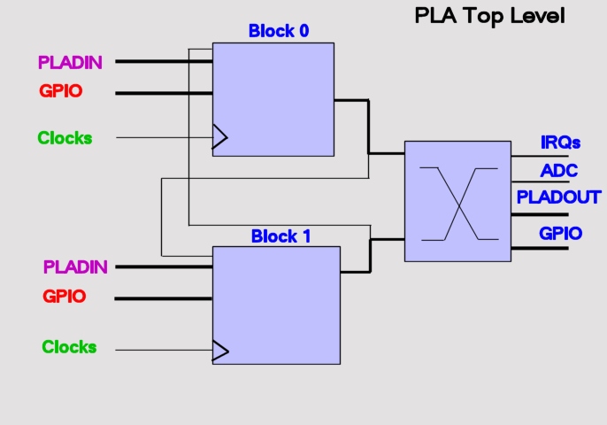
The ADuC7000 Series on chip Programmable Logic Array is organised into two blocks, each consisting of 8 "elements".
As can be seen in the
image above, each block takes inputs from the PLADIN register and from the GPIO pins. Also
visible are the seperate clock lines for each block. There are several clock
sources available e.g. the gpio pins or timer 1. There are individual muxes in
each block allowing the blocks to be clocked by different sources.
The output from the last element of block 0 is also connected as an input to the
1st element of block 1 and vice versa. This interconnection between both blocks
allows the user to avail of all 16 elements in implementing their circuit.
Also visible in the above diagram is the Output Configuration Block. Within
this block the user may choose to select the output of one of the 16 elements
and apply it to IRQ pins or the ADC start conversion signal. By default the
outputs of the 16 elements are available in the PLADOUT register. If the user also
wished the outputs to be available on GPIO pins the they must explicitly enable the pins
via the outputs configuration tab. The
Outputs Configuration block is described in more detail later in the
documentation.