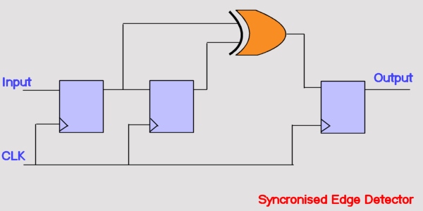
The circuit above is a synchronised edge detector. It re-synchronises the input
to the core clock of the MicroConverter. It then toggles the PLA output each
time the input makes a state transition i.e. low to high or high to low. The
following are the steps the user would take to implement this simple circuit.
Analysing the circuit we see that it contains 3 flip-flops we therefore know it
will require 3 pla elements as each contains a single flip-flop. Launching the
PLA Tool the user can go straight to the block 0 tab and begin to configure the
elements.
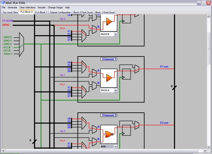
We can see in the image above how the circuit may be implemented. We see
element 0 takes an input from the gpio pins bus which is then passed through
the element's flip-flop. Element 1 then takes an element 0's output as an input
and passed it through its internal flip-flop. Finally the outputs from both
element 0 and element 1 are passed through element 2 where they are exor-ed
together and the resulting output is passed out via element 3's flip-flop. This
mimics exactly the flow shown by the example circuit. Notice that the "HCLK"
input has been selected at the clock source mux, this corresponds to the core
clock.
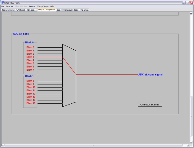
Next we will look at how the output of this signal may be configured to drive
the ADC start conversion signal.
At this point the user can either generate the hexidecimal values for the pla configuration registers or generate ARM or C code to be included in a programming project. We will look at the ARM code produced from this circuit.
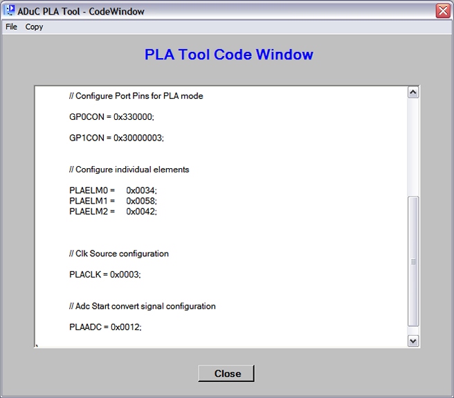
Examining the code we see the first 3 blocks configure the GPIO mux registers
to enable the required GPIO pins in PLA mode. The next three blocks then
configure the individual elements used in the design. Finally code is included
to configure the clock source followed by the adc_st_conv signal.
This example, although trivial, shows how simple the process of designing a
circuit, configuring the pla hardware and producing code can be when using the
PLA Tool.