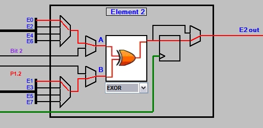
This image shows an element which has been partially configured. In this instance the user has selected an input from element 0 to apply to the even mux and an input from element 1 to apply to the odd mux. The output of these two muxes is then passed through mux A and mux B and are available as the lookup table inputs. The image shows that the user has chosen to apply the "EXOR" function to the inputs and as a result the symbol for an EXOR gate is displayed within the lookup table. By clicking on the combo box below the lookup table the user can choose from 16 different functions. In each case a symbol is loaded to indicate the selected function. Once the function has been selected the output from the table is active as can be seen by the change in color from black to red.
At this point the user has one last decision to make. They must choose whether to pass the input through the element's flip flop there by having it clocked or to bypass the flip flop and pass the signal out directly onto the feedback bus. The flip flops in each element are all clocked by the same source, indicated by a green line in the image. The source is selected at the clock mux shown below.
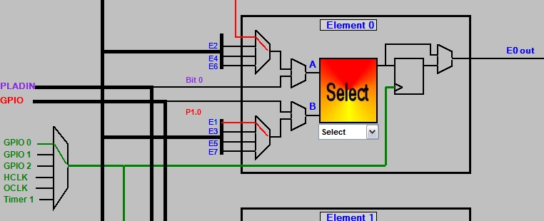
Note in the above configuration the user has chosen the signal on GPIO pin 0 as the clock source for block 0.